品牌/型号:CYT/CYT2305种类:绝缘栅MOSFET沟道类型:P沟道导电方式:增强型用途:SW-REG/开关电源封装外形:SMDSO/表面封装
产品描述
CYT2305是一个使用垂直D-MOS技术的增强型P沟道塑封场效应管这个产品是专门用于计算机,通讯,消费电子以及工业应用等设计中产品特性
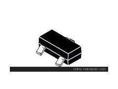
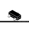
性质:P沟道,中功率频率特性:中频结构:点接触型材料:锗(Ge)封装形式:SOT-23贴片型封装材料:树脂封装类型 | VDSS漏源电压(V) | VGSS栅源电压(V) | ID漏极电流(A) | RDS(导通电阻)(Ω) | PD(耗散功率)(W) | VGS(th)高电平门限(V) | 封装形式 |
P沟道 | -10 | ±12 | -3.5 | 0.045@VGS=-4.5V | 0.55@VGS=–2.5V | 1.25 | -0.45~-1.5 | SOT23-3 |
数据手册 封装,Layout,散热设计
| | |
|
|
|
| |
类型 | P沟道 | VDSS漏源电压(V) | -10 | VGSS栅源电压(V) | ±12 | ID漏极电流(A) | -3.5 | RDS(导通电阻)(Ω) | 0.045@VGS=-4.5V 0.55@VGS=–2.5V | PD(耗散功率)(W) | 1.25 | VGS(th)高电平门限(V) | -0.45~-1.5 | 封装形式 | SOT23-3 |
|
|
| | |
Logic level P-channel enhancement mode Field-Effect Transistor (FET) in a plastic package using vertical D-MOS technology. This product is designed and qualified for use in computing, communications, consumer and industrial applications only. |
|
|
Saves PCB space due to small footprintSuitable for high frequency applications due to fast switching characteristicsSuitable for logic level gate drive sourcesSuitable for low gate drive sources |
Symbol | Parameter | Conditions | Min | Typ/Nom | Max | Unit | VDS | drain-source voltage | Tj ≥ 25 °C; Tj ≤ 150 °C | | | -30 | V | ID | drain current | Tsp = 25 °C | | | -0.52 | A | Ptot | total power dissipation | Tsp = 25 °C | | | 0.417 | W | Dynamic characteristics | QGD | gate-drain charge | VGS = -10 V; ID = -0.3 A; VDS = -15 V; Tj = 25 °C | | 0.5 | | nC | Static characteristics | RDSon | drain-source on-state resistance | VGS = -10 V; ID = -280 mA; Tj = 25 °C | | 0.63 | 0.9 | Ω |
|
|
|
Battery powered applicationsHigh-speed digital interfaces |
|
|
设计与应用 |
|
|
认证和材料报告 |
|
|
此信息由深圳市长运通光电技术有限公司在环球电气网发布,获取优惠采购价格,联系时请说明来自环球电气网!